UV Photodetectors with ZnO Nanowires - Study and Applications
Written by sae-net admin1
Abstract: A comparative study on the photoresponse of zinc oxide nanowires in direct-current (DC) and alternating-current (AC) domains is presented. Zinc oxide ultraviolet photodetectors exhibit positive photoconductivity in DC domain which means that the resistance decreases upon illumination. However, in the frequency domain, zinc oxide nanowires exhibit a solid frequency-modulated response to the ultraviolet illumination leading to a tunable photoconductivity. It is shown that in AC domain the photoresponse of zinc oxide nanowires can be finely adjusted from the positive photoconductivity (resistance decrement) to negative photoconductivity (resistance increment) simply by tuning the driving frequency. Frequency-modulated photoresponse of zinc oxide nanostructures provides an exclusive platform for the realization of dual-response or bipolar photoresponse ultraviolet photodetectors which could be of high technological importance. The zinc oxide nanowires exhibit a responsivity of +180 mA W−1 to the ultraviolet illumination in the DC mode. The nanowires show an almost equal but negative responsivity in the AC domain. Practical implication of the bipolar ultraviolet photodetectors based on ZnO nanowires is presented.
Introduction: Ultraviolet (UV) photodetectors are used in a vast variety of applications including chemical analysis, military warning systems, solar irradiation monitoring, DNA sequencing, optoelectronic converters in photonic array beamformers, and Bragg grating fiber optics in phased array antennas. Although silicon-based UV detectors benefit from mature fabrication technology, their performance is limited to temperatures less than 125 °C. Moreover, since the penetration depth of UV photons into silicon is less than a few tens of nanometers, the depletion region should be formed near the surface of silicon which requires ultra-shallow delta-like doping. Additionally, Si-based ultraviolet photodetectors are very sensitive to a broad range of the electromagnetic spectrum (from mid-UV up to Near-IR) which restricts their application in the presence of visible/solar irradiation. In contrast, wide bandgap semiconductors like group III nitrides and metal oxides are inherently visible/solar-blind, hence providing alternative platforms for exclusive UV detectors.

In recent years, considerable attention has been paid to the optoelectronic applications of wide bandgap metal oxide materials like zinc oxide (ZnO) and titanium dioxide (TiO2). Distinctively, ZnO is one of the most-studied materials for ultraviolet detection because of its chemical stability, low cost, strong radiation hardness, diverse forms of nanostructures, as well as a variety of simple and scalable production methods. Owing to the direct bandgap of 3.3 eV, ZnO only absorbs ultraviolet photons (λ < 400 nm) leading to a high ultraviolet-to-visible rejection ratio. Moreover, zinc oxide and titanium dioxide nanocrystals are very promising for use in optoelectronic devices, including ultraviolet photodetectors, because they benefit from a large surface-to-volume ratio, ultra-high sensitivity, and prolonged photo-carrier lifetime which results in high photoconductive gain.

Experiment: The growth of zinc oxide nanowires is performed in an atmospheric pressure chemical vapor deposition system. A mixture of ZnO nanopowder and graphite (2:1) is used as the deposition seed. The mixture is placed in a ceramic boat and heated at the central zone of the furnace with the approximate temperature of 1100 °C. A constant flow of N2 is introduced into the furnace as a gas carrier. The nanowires were grown on the quartz substrates placed near the end of the furnace where the temperature was around 40 °C. From transmission electron microscope (TEM) analyses, the diameter of individual ZnO NWs is estimated to be 100–150 nm. Selected area electron diffraction pattern of the nanowires matches well with the hexagonal wurtzite structure of zinc oxide.


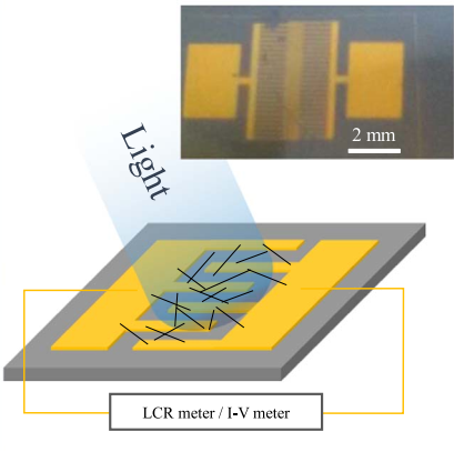
To fabricate the ultraviolet detector, Au is thermally evaporated on the quartz substrates at 10−5 mbar and then patterned into the interdigitated electrodes using standard lithography (distance between adjacent fingers = 100 μm). Then the nanowires were dispersed in methanol (10 mg in 100 ml), ultrasonicated for 20 min, and sprayed on the interdigitated substrates. An optical image and a schematic of device configuration are depicted. GWINSTEK precision LCR meter 821 was used for impedance measurements. In all AC experiments, the DC offset voltage was set to zero. An ultraviolet light emitting diode (LED) with the peak wavelength of 360 nm (FWHM = 10 nm) is used for optoelectronic measurements. The light source switching (i.e., ON/OFF process) was controlled by the input voltage of the LED using MEGATEK MFG-2210P function generator. All the measurements are performed in ambient conditions unless otherwise stated.

Results and Discussion: Au/ZnO/Au metal-semiconductor-metal (MSM) configuration is reported to exhibit both Ohmic and Schottky contacts. In this study, the current-voltage characteristic of Au/ZnO/Au MSM configuration is found to be linear around zero bias which indicates Ohmic MSM contact. Current-voltage characteristic of the ZnO NWs at two different temperatures (26 K and 296 K) shows that at room temperature the current is at least one order of magnitude higher than the current at 26 K indicating thermal activation of carriers into the conduction band of ZnO NWs. Deviation from linear behavior at higher bias voltages comes from the weakly connected nanowires which begin to contribute in current at higher bias voltages.
The current-voltage characteristic of the zinc oxide nanowires in dark and upon ultraviolet illumination are compared. It can be seen that under UV light the current increases at low bias voltages. At higher voltages, the current is governed by series resistance and the device does not exhibit response to UV light. Real-time photoresponse of nanowires (in DC mode) to the ultraviolet illumination with different intensities and various illumination times show that ZnO exhibits positive photoconductivity in DC domain where the resistance decreases upon ultraviolet illumination owing to the generation of excess electron-hole pairs.
In the frequency (AC) domain, the complex impedance plane of nanowires in dark and under UV illumination shows that at low driving frequencies, the resistance decreases upon illumination as observed in DC domain. However, at high driving frequencies the resistance of zinc oxide NWs increases under UV illumination, indicating a negative photoconductivity in the AC domain at high driving frequencies. Real-time AC photoresponse of zinc oxide nanowires at different driving frequencies shows a continuous evolution from positive photoconduction (resistance decrement) at low AC frequencies to negative photoconduction (resistance increment) at high AC frequencies. The tunable polarity of the photoresponse of ZnO NWs in AC domain provides a unique platform for bipolar photo-sensitive detectors based on zinc oxide thin-films and nanostructures.
The fabricated device based on zinc oxide nanowires exhibits a constant responsivity of +180 mA W−1 in the DC mode and an equal but negative responsivity of −180 mA W−1 in the AC mode (200 kHz).
Conclusion: The photoresponse of zinc oxide nanowires upon ultraviolet illumination in direct current and alternating currents domains is investigated. While ZnO nanowires display positive photoconductivity in DC domain, they may exhibit positive or negative photoconductivity in AC domain depending on driving frequency. The frequency-modulated tunable photoresponse of zinc oxide nanowires is explained based on the surface conduction channel provided by negatively charged oxygen molecules. This tunable photoconductivity in AC domain can be utilized to develop switchable bipolar ultraviolet photodetectors. The device characterization procedure was carried out over 4 weeks and demonstrated good stability of the fabricated device.